For six decades, the semiconductor industry has followed a simple playbook: shrink transistors, pack more onto a chip, repeat. That formula is running into physics. Transistors are now so small that quantum effects start to interfere. The next move, researchers have long argued, is to build upward.
A team at the University of Illinois Urbana-Champaign, led by materials science professor Qing Cao, has demonstrated a way to do exactly that. Their research, published in Nature in late May, details a method for stacking multiple layers of silicon circuits directly on top of one another using standard single-crystalline silicon. The results suggest the approach could eventually be adopted by commercial chip manufacturers.
The thermal problem
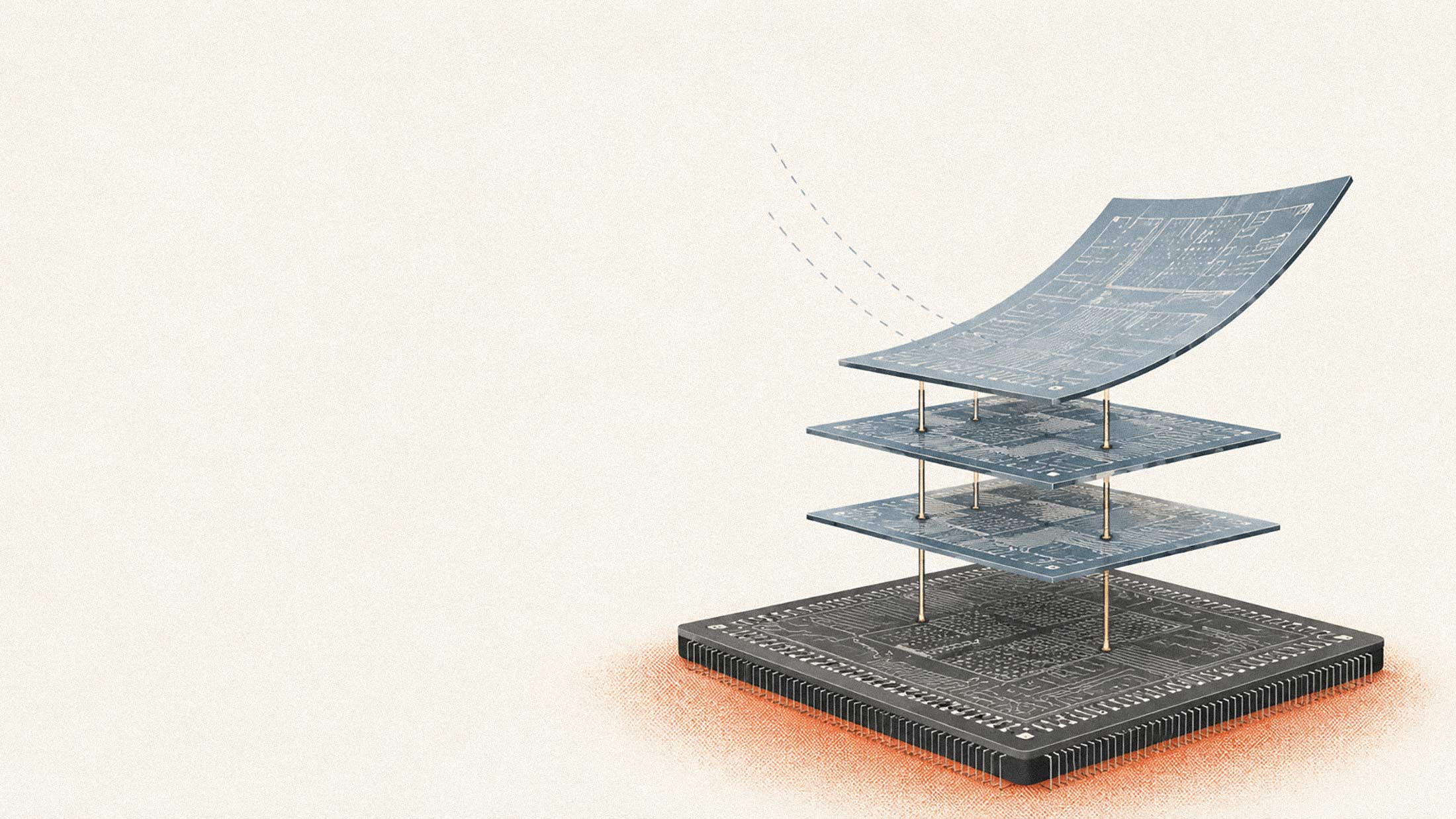
Building circuits vertically sounds straightforward until you consider heat. Manufacturing traditional silicon transistors requires temperatures exceeding 1,000°C. At those temperatures, any circuitry already on the chip would be destroyed. Previous attempts at monolithic 3D integration have relied on exotic materials like carbon nanotubes or metal-oxide semiconductors. These work, but they sacrifice the performance characteristics that make silicon the industry standard.
Cao's team found a workaround. They use extremely thin, flexible sheets of silicon just 10 nanometers thick, peeling them from a specialized substrate using adhesive tape. A roller then transfers these membranes onto the chip at temperatures below 200°C, well within safe limits for the layers beneath. The sheets conform to surface imperfections, producing a uniform bond even when the underlying topography is uneven.
Performance that matters
Using this technique, the researchers built three stacked silicon layers containing 625 transistors each. Device yields ranged from 98 to 100 percent, and performance was comparable to conventional silicon transistors fabricated at much higher temperatures. The team also demonstrated 3D logic circuits and static random-access memory cells by connecting the layers with vertical metal links.
The process is scalable, according to Cao. Additional layers can be stacked beyond the three demonstrated in the study. The researchers are now working to transfer the technology into industrial foundries, with support from IBM, Intel, and TSMC.
Why it matters now
Vertical integration is already appearing in commercial products. AMD's MI300 series, for instance, stacks prefabricated layers on top of each other using metal pillars called through-silicon vias. But this approach limits the density of connections between layers. Monolithic integration, where transistors are built sequentially on a single wafer, removes that constraint. The Illinois work is among the first to achieve this with production-grade silicon.
The timing is relevant. Demand for AI compute has pushed the semiconductor market into hypergrowth. Deloitte now estimates the AI chip market will reach approximately $500 billion in 2026, driven by appetite that traditional scaling cannot satisfy. Building upward offers a path to higher transistor density without requiring breakthroughs in lithography or new materials.
Meanwhile, AI is reshaping how chips are designed in the first place. Machine learning now handles yield optimization, defect detection, and process control in fabrication. Verification, which accounts for up to 70 percent of design effort, is increasingly automated by pattern-recognition systems trained on databases of known flaws. The loop is tightening: AI accelerates chip design, and those chips accelerate AI.
The Illinois research does not solve every problem. Thermal management in densely stacked circuits remains a concern. So does the cost of scaling the roll-transfer process to 300mm production wafers. But the work demonstrates that the physics of monolithic 3D integration are tractable, and that silicon, the material the industry already knows how to use, can be part of the solution.