Huawei made a bold claim today at the IEEE International Symposium on Circuits and Systems in Shanghai: it can close the gap with TSMC without the advanced lithography equipment it has been blocked from buying.
In a keynote speech titled "New Semiconductor Path in Practice," He Tingbo, president of Huawei's semiconductor business and chair of its Scientist Committee, introduced what the company calls the Tau (τ) Scaling Law. The core idea: instead of shrinking transistors further, optimize for the time it takes signals to move through a chip and its surrounding system.
A Different Kind of Scaling
Moore's Law, which has guided chipmaking for more than five decades, is hitting physical and economic walls. Huawei's proposal sidesteps this by targeting signal propagation delay rather than geometric miniaturization. The company says this allows it to improve chip performance and density through circuit design and advanced packaging, rather than relying on the cutting-edge EUV lithography machines from ASML that US export restrictions have placed off-limits.
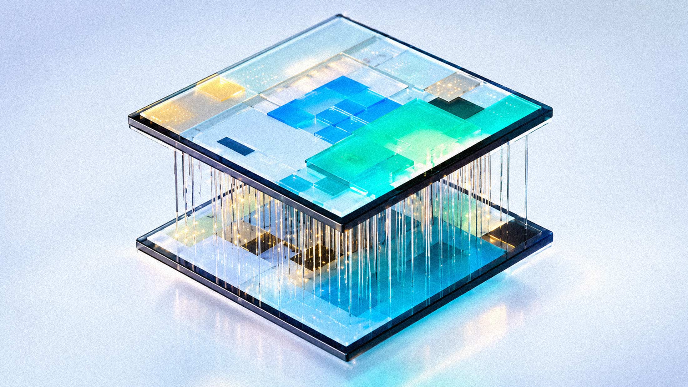
The flagship implementation is an architecture Huawei calls LogicFolding. According to technical analyses, the approach distributes logic gates across stacked wafer layers connected by ultra-fine hybrid bonding, allowing signals to travel vertically through tens of micrometers instead of routing horizontally across hundreds of micrometers or more. Shorter paths mean lower resistance and capacitance, which compresses timing delays.
The principle has already earned a nickname in industry circles: "Her's Law," a play on He Tingbo's surname and the tradition of naming scaling laws after their originators, according to the South China Morning Post.
The Roadmap
Huawei says it has already designed and mass-produced 381 chips over the past six years using aspects of the Tau Scaling approach, spanning smartphones and AI computing. The next milestone is the fall 2026 Kirin chip lineup, which will be the first to fully adopt LogicFolding architecture.
By 2031, Huawei expects its high-end chips to feature transistor density equivalent to 1.4-nanometer processes. That target is noteworthy because TSMC, the world's leading contract chipmaker, plans to begin mass production of its own 1.4nm process in 2028. Today, according to Bloomberg, there is roughly a five-year gap between what TSMC can produce and what Huawei, working with manufacturing partner SMIC, is capable of.
If Huawei hits its 2031 target, it would narrow that gap to approximately three years. A meaningful reduction, though not parity.
What Huawei Didn't Say
The company provided no independent verification of its performance claims. Design targets and manufacturable silicon at scale are different things, and the distinction matters. SMIC, which fabricates Huawei's most advanced chips, remains stuck at 7nm-class production and has struggled with yields on its 5nm-like process. Moving to density-equivalent architectures through packaging tricks does not solve the underlying manufacturing constraints.
Still, Huawei's semiconductor ambitions have exceeded skeptics' expectations before. In 2023, the company surprised the industry with its 5G-capable Mate 60 smartphone, powered by a Kirin chip produced at SMIC using 7nm technology. That launch came after years of predictions that US sanctions would cripple Huawei's mobile hardware business.
The Competitive Context
Nvidia CEO Jensen Huang recently acknowledged that his company has "largely conceded" China's AI chip market to Huawei. The Chinese firm is targeting shipments of 750,000 AI chips in 2026, with expected revenue of $12 billion from AI chips alone. Whether Huawei's architectural innovations can compensate for its manufacturing disadvantages remains an open question.
He Tingbo closed her keynote by calling for industry collaboration. "We believe that openness and collaboration are key to driving ongoing progress in the semiconductor industry," she said. "No single company can independently find all the answers along the path of semiconductor evolution."
The statement carries some irony, given that Huawei's entire research program exists because collaboration with Western suppliers is no longer an option.