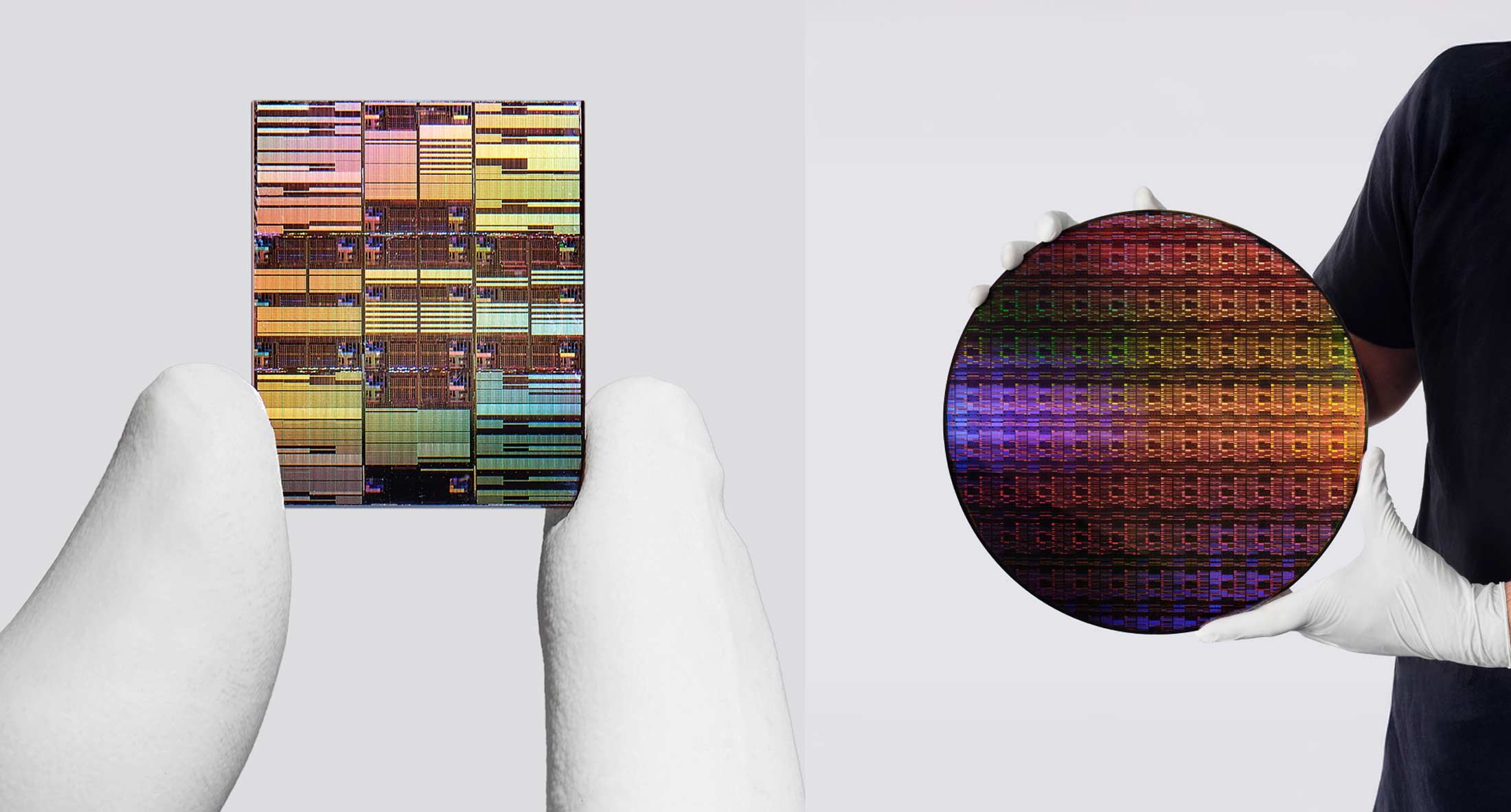
IBM today announced what it calls the world's first sub-1 nanometer chip technology, built on a novel three-dimensional transistor architecture the company has named nanostack. The announcement marks a symbolic threshold: transistors have now entered the angstrom era, where dimensions approach the scale of individual atoms.
The new 0.7nm node, also referred to as 7 angstroms, can pack nearly 100 billion transistors onto a chip the size of a fingernail. That's roughly double the transistor density IBM achieved with its 2nm chip, which the company unveiled in May 2021 and which has since been adopted by Intel, Samsung, and TSMC for mass production. IBM projects the new technology will deliver up to 50 percent better performance or 70 percent greater energy efficiency compared to those 2nm chips.
What Nanostack Actually Does
The core innovation here is structural. Rather than laying transistors flat, nanostack vertically stacks and staggers them across two separate wafers, connected by an ultra-thin dielectric bond. Each transistor in the stack can use different channel materials, allowing designers to independently optimize performance and power consumption for each layer.
"We have entered a domain in semiconductor manufacturing that works between magic and physics," said Huiming Bu, VP of IBM Semiconductors Global R&D;, during a press briefing.
This is a departure from IBM's previous nanosheet technology, which the company invented and which became the industry's leading-edge transistor architecture. Nanosheet replaced FinFET designs and enabled the 3nm and 2nm generations. Nanostack extends that approach into three dimensions.
The architecture was experimentally validated through functional CMOS inverter operation, a basic building block in digital chips. IBM researchers also demonstrated a 40 percent improvement in SRAM scaling, a result presented at VLSI 2026. For AI workloads that depend on high-bandwidth, low-latency memory, that improvement matters significantly.
The Timeline Question
IBM expects the earliest commercial adoption of nanostack chips within five years. The company has not named a manufacturing partner for the sub-1nm technology, though it currently works with Japan's Rapidus on 2nm production and uses Samsung as a foundry supplier for existing designs.
The research is being conducted at IBM's Albany, New York semiconductor facility, where the company is installing a High Numerical Aperture Extreme Ultraviolet lithography tool from ASML. High NA EUV is considered essential for the next generation of logic scaling.
IBM believes nanostack can sustain at least a decade of additional scaling, a claim that carries significant weight as the industry approaches what many have long considered the physical limits of conventional chip manufacturing. Jay Gambetta, Director of IBM Research, characterized the announcement as pushing technology "beyond the nanometer era to the scale of atoms."
Context and Competition
IBM's position in semiconductors is unusual. The company sold its microelectronics manufacturing unit to GlobalFoundries in 2014 but retained its research operation, which has continued producing landmark demonstrations that others license and commercialize. The 2nm chip followed this pattern, with technology developed in Albany eventually appearing in products from foundries around the world.
The sub-1nm announcement arrives as competitors are also pursuing advanced nodes. TSMC, Samsung, and Intel have all signaled aggressive roadmaps. But IBM's approach, which emphasizes architectural innovation over brute-force shrinking, suggests the company sees vertical integration as the path forward.
To put 7 angstroms in perspective: a human red blood cell is about 7,000 nanometers wide. A glucose molecule is roughly the width of one of these new transistors. At these scales, the distinction between engineering and physics starts to blur.
Whether IBM can translate laboratory results into commercial products in a competitive timeframe remains to be seen. Five years is a long time in semiconductors. But the company's track record on fundamental research is difficult to dismiss.