Every semiconductor chip begins the same way: a pattern of light, projected onto silicon, defining what the chip can become. This process has a name that sounds simple and isn't. Lithography. It accounts for roughly 30 percent of wafer processing costs. It determines which transistors are possible at which price points. And at the bleeding edge, it is controlled almost entirely by one company in the Netherlands.
Drawing With Light on Stone
Lithography, derived from the Greek for "drawing with light on stone," works through repetition. A wafer is coated with photoresist, a light-sensitive polymer. A mask containing the circuit pattern is placed above it. Light passes through the mask and changes the chemical structure of the resist, which can then be etched away to create the shapes that eventually become transistors, wires, and the billions of interconnects that let modern processors think.
This cycle repeats dozens of times per chip. Advanced processors can have more than 100 layers, each requiring its own mask, its own exposure, its own etching step. A single CMOS wafer may go through the photolithographic cycle 50 times before it's finished.
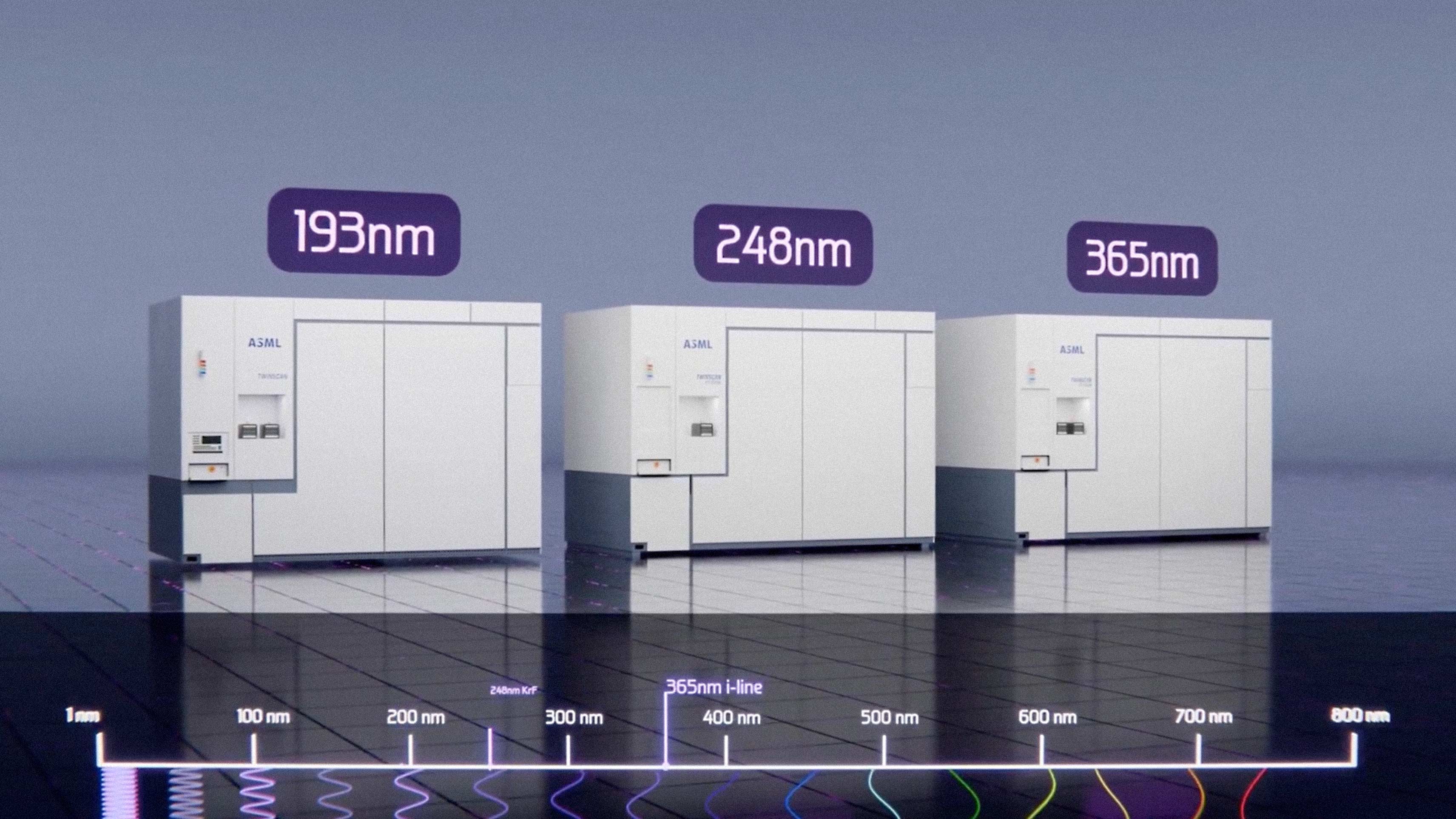
The key variable is wavelength. Shorter light waves can draw finer lines. For decades, the industry pushed mercury vapor lamps and then excimer lasers into shorter and shorter wavelengths: 436 nanometers in the 1970s, 365nm by the mid-1980s, then 248nm and finally 193nm by the late 1990s.
The DUV Era and Its Tricks
Deep ultraviolet lithography at 193nm remains the industry's workhorse. ZEISS, which manufactures the optics for most of these systems, notes that more than 95 percent of chip structures are still created with DUV light at wavelengths of 193, 248, or 365 nanometers. By the mid-2000s, engineers introduced immersion lithography, filling the gap between lens and wafer with water to increase the numerical aperture and push resolution below 40 nanometers.
But physics imposes limits. At some point, 193nm light simply cannot resolve smaller features without tricks. Enter multi-patterning: exposing the same layer multiple times, shifting the mask slightly, layering the results. A line that cannot be drawn in one pass can be constructed in two or four. Chinese foundries still use this approach to produce chips at 7nm and even 5nm without EUV access. It works. It is also slow, expensive, and prone to errors.
The real reason cutting-edge fabs still use DUV tools alongside their newest machines is economics. A chip consists of critical layers, where transistors live, and less demanding upper layers, where wider metal interconnects run. EUV tools typically pattern the critical layers. DUV handles the rest. Most advanced fabs operate intricate ecosystems of different lithography tools, matching each layer to the appropriate wavelength and machine cost.
Extreme Ultraviolet: A 20-Year Bet
The AI revolution runs on chips that could not exist without EUV lithography. ASML, headquartered in Veldhoven, is the only company on earth that manufactures these machines for commercial production. Its EUV systems use light with a wavelength of 13.5nm, roughly one-fourteenth the wavelength of DUV. This allows single-exposure patterning at scales that would require multiple DUV passes.
The technology took more than two decades to develop. ASML's first EUV prototype in 2006 produced one wafer in 23 hours. Today's scanners process over 200 wafers per hour. The breakthrough required reinventing nearly everything. EUV light is absorbed by air, so the entire optical path must operate in a near-perfect vacuum. Conventional lenses absorb EUV, so the system uses mirrors instead, manufactured by Zeiss to sub-atomic precision. The light source itself comes from firing 50,000 molten tin droplets per second through a chamber, vaporizing each with a CO2 laser to create plasma hotter than the sun's surface.
Standard EUV systems cost around $180 million each. ASML shipped over 100 of them by early 2020 and now targets 60 units for 2026 alone. The company's market capitalization exceeds $500 billion.
High NA and the Angstrom Era
The next generation is already arriving. High-NA EUV systems, ASML's EXE platform, increase the numerical aperture from 0.33 to 0.55. This enables resolution down to 8nm in a single exposure, enough to manufacture chips at 2nm and below. These machines cost around $380 million each. They weigh 150,000 kilograms. They ship in 250 crates and require six months and 250 engineers to assemble.
Intel received the first commercial High-NA tool at its Oregon fab in early 2024 and is now using it to develop its 18A (1.8nm-class) process. Samsung has secured its own EXE:5200B systems for 2nm logic and advanced memory production. TSMC, interestingly, has indicated it may skip High-NA for its initial 1.4nm node, betting that multi-patterning on existing EUV tools can stretch further before the capital investment is justified.
Imec, the Belgian research consortium, announced in March 2026 that it had received and installed an EXE:5200 unit. Fewer than a dozen exist globally. The system enables chip features up to 66 percent smaller than previous EUV generations.
The Machines That Make the Machines
The geopolitics here are obvious but worth stating. ASML depends on over 5,100 suppliers spanning multiple continents. Cymer, now an ASML subsidiary, builds the laser systems in San Diego. Zeiss manufactures the mirrors in Germany. The EUV LLC consortium, formed in the late 1990s with backing from Intel and the U.S. Department of Energy, funded much of the early research. This is why U.S. export controls apply to ASML's machines despite the company being Dutch.
China has no access to EUV equipment. Reuters reported in December 2025 that a prototype EUV system was secretly completed in Shenzhen, expected to produce working chips between 2028 and 2030. Whether this changes the strategic picture remains unclear. ASML's lead is measured in decades of accumulated engineering, not just patent filings.
Future Generations
ASML has already announced plans for Hyper-NA EUV, with a numerical aperture of 0.75 or higher, targeting sub-1nm nodes sometime after 2028. Each generation demands new masks, new resist chemistries, new metrology tools. The AI supercycle is driving unprecedented demand for the most advanced chips, and ASML's order backlog now exceeds $46 billion.
The cost curve is concerning. High-NA machines consume several megawatts of power each, requiring dedicated utility substations. The extreme capital requirements mean only a handful of companies can afford to operate at the leading edge. This concentrates advanced chip production in ways that have implications for national security, industrial policy, and the long-term structure of the computing industry.
For now, every advanced AI model, every smartphone processor, every data center GPU exists because of light projected through masks onto silicon. The wavelength keeps shrinking. The machines keep getting more expensive. And one company in the Netherlands keeps building them.